STEM outreach events often include a combination of presentation style and hands-on activities, and perhaps a chance to look into a working lab, if the event includes a site visit to Georgia Tech’s campus.
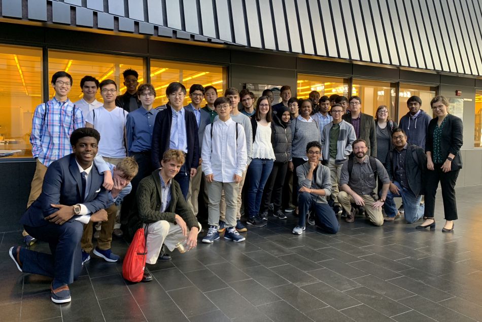
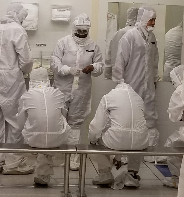
Sophomore level students from the Gwinnett School of Mathematics, Science, and Technology (GSMST) got the rare chance to “gown up” and enter the research cleanrooms at the Marcus Nanotechnology Building, home of the Institute for Electronics and Nanotechnology at Georgia Tech. This “gowns-on” approach to outreach was planned by Professors Asif Khan and Azadeh Ansari, both of the School of Electrical and Computer Engineering (ECE), and Ms. Nicole D’Antonio, Partnership & Internship Coordinator at GSMST.
Prof. Khan gave the welcome note and explained that the brains of our electronic gadgets, the chips, are made in the clean room by showcasing a 300 mm silicon wafer and a video on how sand is transformed into silicon chips.
When asked about their favorite part of the site visit there was a definite theme:
- “…putting on the clean room suits and touching the pure gold…”
- “The best part was going into the clean room looking like I was about to go to space. I had never thought about how clean an environment needs to be so that the chips that go into our phones and computers can be properly processed.”
- “The best part of the visit was actually preparing to enter the clean room. I would have never guessed a person would have to wear a lot of protective gear to prevent the releasing of particles in the air.”
- “I personally loved this trip because this experience helps me see my possible future major, and even school!”
Georgia Tech is proud to be the primary location of the Southeastern Nanotechnology Infrastructure Corridor (SENIC), one of the sites in the National Science Foundation’s (NSF) National Nanotechnology Coordinated Infrastructure (NNCI), as well as the home of the NNCI Coordinating Office.